Smaller, faster, more energy-efficient
High-performance devices for digital transformation
Highly efficient power semiconductors are to pave the way for a wide range of novel applications – from e-mobility to artificial intelligence. This is the objective of the recently launched joint project “power transistors based on AlN (ForMikro-LeitBAN)” coordinated by the Ferdinand-Braun-Institut and in which FAU Engineers are involved.
Smart energy supply, electro-mobility, broadband communication systems and applications of artificial intelligence (AI) – the number of interacting and interconnected systems is constantly growing. At the same time, the responsible use of resources is a crucial social challenge. With a growing number of systems and increasing data traffic primary energy consumption is also on the rise. Electrical energy must be converted at all times to be usable by the various systems, which is why the need for electrical conversion is also increasing. In Europe alone, it is estimated that more than three terawatt hours of energy are lost by energy conversion each year – the amount of electricity produced by a medium-sized coal-fired power plant. The efficient conversion of energy is therefore critical for applications like AI and IIoT or Industry 4.0 − the digitalisation of manufacturing. ForMikro-LeitBAN is investigating technology that can increase efficiency and conserve valuable resources. This requires efficiently switching power semiconductors that enable a high power density. Used to a large extent, this would result in noticeable energy savings and make a relevant contribution to CO2 reduction.
The project aims at developing aluminium nitride as the new semiconductor material for this task, to test it with suitable devices and to qualify it for future applications in systems. Until 2023, the project will be funded with 3.3 million euros by the Federal Ministry of Education and Research within the ForMikro programme.
Aluminium nitride – starting material with potential
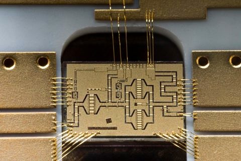
The efficiency of systems is limited by static and dynamic power losses of semiconductors, determined by the respective material. It is becoming increasingly difficult to increase the efficiency of electrical converters and power amplifiers with conventional silicon-based power components. New semiconductor materials with improved properties must therefore be investigated and brought to market maturity. The project partners rely on aluminium nitride (AlN). This semiconductor material, which has so far received little attention in for electronic applications, offers up to 10,000 times less conduction losses than silicon devices. It is also characterised by very high breakdown strengthand thermal conductivity – ideal prerequisites for power semiconductors with high energy density and efficiency. Free-standing insulating AlN wafers are to be used and qualified as the material basis. Compared to AlN epitaxy on foreign substrates such as silicon carbide, the dislocation density can be reduced by five orders of magnitude. This offers the potential for fast and efficient switching devices while maintaining high reliability.
Full process chain – from crystal growth to system demonstrators
From a conceptual point of view, the novel AlN components are based on the well-researched GaN technology. A new aspect is the transition from conventional foreign substrates such as silicon carbide, sapphire or silicon to free-standing AlN substrates. ForMikro-LeitBAN researches the development of such AlN wafers and tests them in a tailor-made device process. Test systems for millimetre wave applications and for power electronic energy converters qualify the new highly efficient AlN devices for applications in corresponding systems. Researchers will prepare the transfer of this technology into an industrial environment in a follow-up project. An industrial advisory board supports the consortium’s work: Infineon for power electronics, UMS for millimetre wave technology and III/V-Reclaim for the recycling of AlN wafers.
The following partners are involved in ForMikro-LeitBAN and jointly cover the entire value chain – from AlN wafers to both millimetre waves and power electronic systems:
- Ferdinand-Braun-Institut (FBH): AlN device design and development
- Fraunhofer IISB, Erlangen (IISB): AlN crystal growth, wafer manufacturing
- TU Bergakademie-Freiberg (IAP): Process module development, analytics
- Friedrich-Alexander-Universität Erlangen-Nürnberg (FAU): material analysis
- Brandenburgische Technische Universität Cottbus-Senftenberg (BTU): AlN millimetre wave systems
- Technische Universität Berlin (TUB); AlN power electronic systems
Further Information
www.elektronikforschung.de/projekte/formikro-leitban
Dr. Elke Meissner
Tel.: 09131/85-28634
elke.meissner@fau.de